
Introduction
Parity bits are extra signals which are added to a data word to enable error checking. There are two types of parity – even and odd. An even Parity Generator will produce a logic 1 at its output if the data word contains an odd number of 1s. If the data word contains an even number of 1s then the output of the Parity Generator will be 0. By concatenating the parity bit to the dataword, a word will be formed which always has an even number of 1s i.e. has even parity.
Parity is used on communication links (e.g. modem lines) and is often included in memory systems. If a dataword is sent out with even parity, but has odd parity when it is received then the data has been corrupted and must be resent. As its name implies the operation of an Odd Parity generator is similar but it provides odd parity. The table shows the parity generator outputs for various 4-bit data words.
Objectives
- Use a Truth Table to construct odd parity generator.
- Derive the logic circuit from algebraic function obtained from Truth Table
- Design and simulate the Parity Generator in NI Multisim 13.0
- Implement the Parity Generato on a Digilent Basys 2 Spartan-3E FPGA board
Hardware Requirements
Digilent Basys2 Spartan-3E FPGA Board (the board comes with an USB programming cable)

Software Requirements
- NI Multisim 13.x Education Edition (to download an evaluation edition, please click here)
- ISE WebPACK Design Software (available here)
- Xilinx iMPACT 13.x or later, part of the ISE WebPack (link as shown in previous line)
Installation Instructions
- Download the attached Digilent Basys 2 file.
- Unzip the file to your local disk.
Two files will be unzipped: DigilentBasys2.mspc and DigilentBasys2.ucf.
- Copy and paste the two unzipped files to the pldconfig folder in the main Multisim 13.0 install directory, by default, this should be:
Program Files->National Instruments->Circuit Design Suite 13.0->pldconfig
In my PC it looks like as show using WinRAR (evaluation copy):

Pressing OK the files will be duly copied.
Procedure
A) Derive the Logic Circuit of 4-Bit Parity Generator
The Truth Table of 4-Bit Parity Generator is:

The equivalent Karnaugh Map (K-Map) is:

From K-Map, we can derive the algebraic function which is (P is the parity result):
P = A’B’C’D+A’B’CD’+A’BC’D’+A’BCD+AB’C’D’+AB’CD+ABC’D+ABCD’
This result can be simplified as:
P = A’B'(C’D + CD’) + A’B (C’D’+CD) + AB'(C’D’ + CD) + AB (C’D + CD’)
= (A’B’ + AB) . (C’D + CD’) + (A’B + AB’) . (C’D’ + CD)
P is the result in our case for Odd Parity.
We note that above algebraic simplification is representing XOR (short for Exclusive-OR) and XNOR (short for Exclusive-NOR) gates. You can read an excellent tutorial here.
Hence:
P = (A ⊕ B)’ . (C ⊕ D) + (A ⊕ B) . (C ⊕ D)’
= (A ⊕ B) ⊕ (C ⊕ D)
This algebraic function is represented by following logic circuit:

B) Design the Schematic and Simulate
We will first design the top level schematic in NI Multisim 13.0 which is used for simulation purposes and contains the PLD subsheet.
The top level schematic, as part of this project, allows for simulation. It places the PLD logic in place around the IO contained on the board. To achieve this we use a PLD sub-circuit. The PLD sub-circuit allows us to place the PLD code within a single component as if it was being run on the FPGA.
The steps below describe the process for creating a sub-circuit.
1. Open a new schematic in Multisim.
2. Select Place » New PLD sub-circuit
 3. Choose Digilent Basys 2 and click Next button

4. Provide a name for the PLD schematic. I chose “Parity Generator”, as can be seen in image, leaving the default PLD part number as it is:
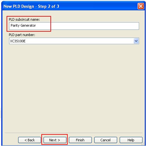
5. Select the connectors that you will be using on the Basys 2 Spartan-3E FPGA board. For the Parity Generator in this tutorial we will be using:
sw_0, sw_1, sw_3 and sw_4 for simulating input values A, B, C and D respectively on Basys 2 FPGA board. Led_0 for output on the Basys 2 board and to indicate Odd Parity.
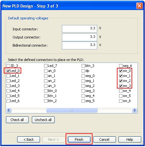 We will keep all other default values as they are, and click Finish button.
6. Place the sub-circuit
The sub-circuit is created:
 Save the Multisim schematic giving it a name. I have called it “my_Parity_Generator”.
After completing the top level circuit, we need to create the digital logic within the PLD schematic. We will next edit the sub-circuit and connect it up.
To create the PLD schematic right-click the PLD sub-circuit and select Properties. A window will pop up:

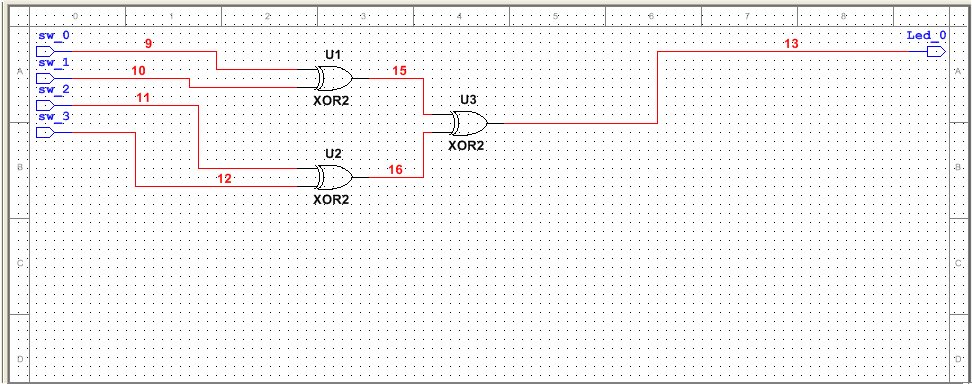
Click Open subsheet button. An empty schematic with connectors for sw_0, sw_1, sw_3, sw_4 and Led_0
Connect up the logic circuit obtained before as shown:
 Save the circuit.
7. Simulating the Logic
The top-level schematic can be simulated by adding a Logic Analyzer and a Word Generator as shown:
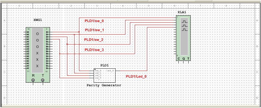
Set up the Word Generator first. Doube-click on XWG1.
Settings window will pop up. On Display group of options choose Binary

Controls group of options click Set… button

Choose up counter and keep the default Initial pattern.

Up counter will be generated. We will now limit at 1111. Click on this pattern and right-click with mouse and choose Set Final Position.

Now double-click on XLA1, Logic Analyzer. On Word Generator click the Step button. As you Step through the patterns you will see the Logic Analyzer displaying the patterns as well the Parity result.
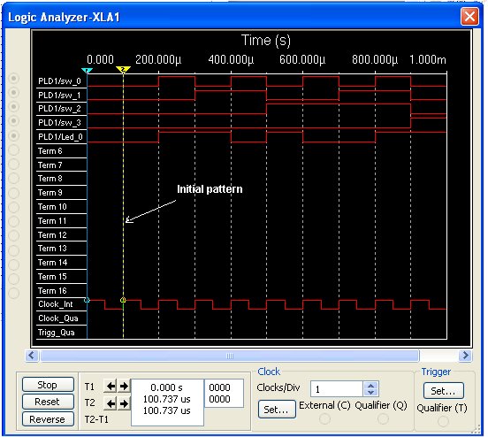
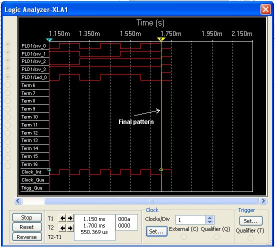
You can verify the Truth Table for Odd Parity outputs:
In fact Even Parity is inverse of Odd Parity, therefore in our PLD sub-circuit we could have also obtained this result by just placing an Inverter at output.
We can also test the circuit by connecting a LED to the output of PLD, and by stepping through the patterns in Word Generator. Everytime the LED is ON it means that it is Odd Parity.
8. Deploying the Logic
There are three options for exporting the digital logic from the PLD schematic:
– Programming the connected Hardware – allows students to deploy the digital logic and learn the response of using the hardware.
– Generate a PLD bit file – students can take this away and deploy when they have the hardware available.
– Generate VHDL file – allows students to explore the VHDL behind the logic.We will focus on programming the connected hardware.
NOTE: If your Windows OS is not in english language, you will need to edit the TEMP and TMP localization in My Computer -> Properties -> Advanced -> Environment Variables. You will have to change it from %USERPROFILE%\Local definitions to %SYSTEMROOT% to avoid XST Synthesis failure. This happens as the command lines of compilation do not accept foreign language characters such as ç, õ and others of similar nature . Of course you will need to restart your PC, after having made these changes to your Windows’ Environment Variables.
Right-click the PLD sub-circuit and select Properties. A window will pop up:
Click Open subsheet button. The logic circuit that we designed before will be shown:
- Make sure that your Basys 2 board is connected to your PC with USB cable that comes with it.
- Select: Transfer » Export to PLD from the menu bar.

- Here you will see the three export options. We want to export to physical hardware so select Program the Connected PLD.
 We want to program the connected PLD. Click Next.
 In my Windows environment I have already installed Xilinx ISE Design Suite 14.2. Note that Device Status is not checked. Make sure first of all that Basys 2 board is connected. You may need to install Adept software and make sure that the board is recognised by your PC.
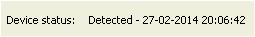
- Click on Refresh button. Multisim will try to detect the Basys 2 FPGA board. Note that Multisim 12.0 does not detect the board.
 If detected you will see the following reassuring information on this step.
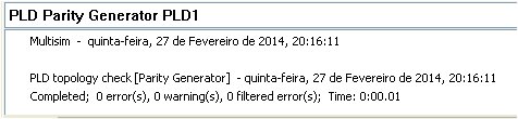
- Now click Next. You will see first of 11 steps that Multisim 13.0 will go through
 If all goes well your Basys 2 FPGA board (or any other supported Digilent boards such as Nexys 2 and 3 – you will need to install in Multisim the adequate constraints files) , you will see the following reassuring result:
 9. Testing the logic
On Basys 2 FPGA board test the logic by switching HIGH and LOW the switches sw_0, sw_1, sw_2 and sw_3, and confer with the Truth Table by the Led_0 being lit (in HIGH state) or not (in LOW state):


Conclusions
A parity bit is used for the purpose of detecting errors during transmission of binary information. We have used two excellent tools NI Multisim and Digilent Basys 2 FPGA board. We first derived the logic circuit of 4-Bit Parity Generator from the Truth Table, simulated the derived circuit in NI Multism, and then finally implemented it physically on a Digilent Basys 2 FPGA board.
Acknowledgments
(1)http://www.webopedia.com/TERM/P/parity_checking.html

The XOR circuit shown is for even parity generator as it generates a 1 when there are odd number of 1s in the input??truth table is not matching with the explanation of parity generator unless using a negative logic. pls clarify.
The truth table shows you can generate odd or even parity. You can choose whatever parity generation you want.
Isn’t the XOR circuit shown in the figure generating an even parity bit?( output shown as odd parity in the figure)
Please read the tutorial to end. It is quite clear that you just need to invert.